NXP ADC/DAC PCF8591 (I2C)
Jump to navigation
Jump to search
File:TArduinoPCF8591ADCDAC.png
Summary
I²C 4-channel 8-bit ADC with 1-channel 8-bit DAC. Provides analog input/output expansion.
Description
Monolithic data acquisition device with 4 analog inputs configurable in multiple single-ended and differential modes, 1 analog output, and serial I²C interface. Three address pins allow up to 8 devices on the same bus. Sample rate ~3-11 kHz. Typical applications: sensor monitoring, analog signal generation, and I²C bus expansion.
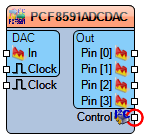
Diagram:
Properties
- Address – I²C device address (Default: 0x48)
- Mode – Configures the ADC input channel operation mode.
* Options: adcSingleEnded, adc3Differential, adcMixed, adc2Differential; Default: adcSingleEnded
- DAC Enabled – Enables the analog output (Default: True)
- DAC Initial Value – Startup output value 0-255 (Default: 0)
Pins
Input Pins
- DAC Group
   *In (analog) – Analog input signal to be converted.
   *Clock (digital) – Clock input for the conversion timing.
- Clock (digital) – Master clock input for the component.
- Control (i2c) – I²C control bus (SDA, SCL) for communication and configuration.
Output Pins
- Pins Out Group
   *Pin [0] (analog output)
   *Pin [1] (analog output)
   *Pin [2] (analog output)
   *Pin [3] (analog output)
